A Primer on Semiconductor Capital Equipment (Semicap)

The semiconductor capital equipment (semicap) industry is one of the most important industries on the planet and one that doesn’t get much love (outside of ASML). The industry has a number of structural advantages leading towards attractive investment characteristics for long-term, quality-focused investors: deep competitive advantages, technical differentiation, strong returns on capital, and high amounts of cash returns to shareholders.
For those who have been reading my work for a long time, you know I’ve been heavily influenced by the value-investing school of thought. One of my beliefs is that looking for the highest-quality technology companies with deep competitive advantages will yield outperformance over time.
The large semicap companies have some of the deepest competitive advantages in technology, leading to them operating in monopolies or oligopolies. The primary risks are cyclicality, geopolitical concerns, and the analytical rigor involved with investigating those two variables. The industry isn’t for those who lack conviction.
My goal for this article is to provide an introductory piece on the semiconductor manufacturing process, the semicap markets, and the trends diving this industry. I’ll then dive deeper into individual companies in future articles.
I’ll be structuring the article as follows:
- Background on the Semiconductor Industry
- An Overview of the Semiconductor Manufacturing Process
- An Overview of the Semicap Market
- Public Comps Data
- Final thoughts on the Space
Disclaimer: the technology of semicap is exceptionally complex. I don’t pretend to be an expert on the technology, just a student of the space. Two of the best resources for further reading are SemiAnalysis and Fabricated Knowledge (feel free to add others in the comments).
Disclaimer x2: I admire the competitive advantages of the semicap companies, and I think several are wonderful businesses. That doesn’t mean they are always great investments (i.e. valuation). This article is mostly positive towards the large semicap businesses, but everyone should do their own due diligence on valuation.
1. Background on Semiconductor Markets
The semicap industry is ultimately driven by the overall growth of the semiconductor market.
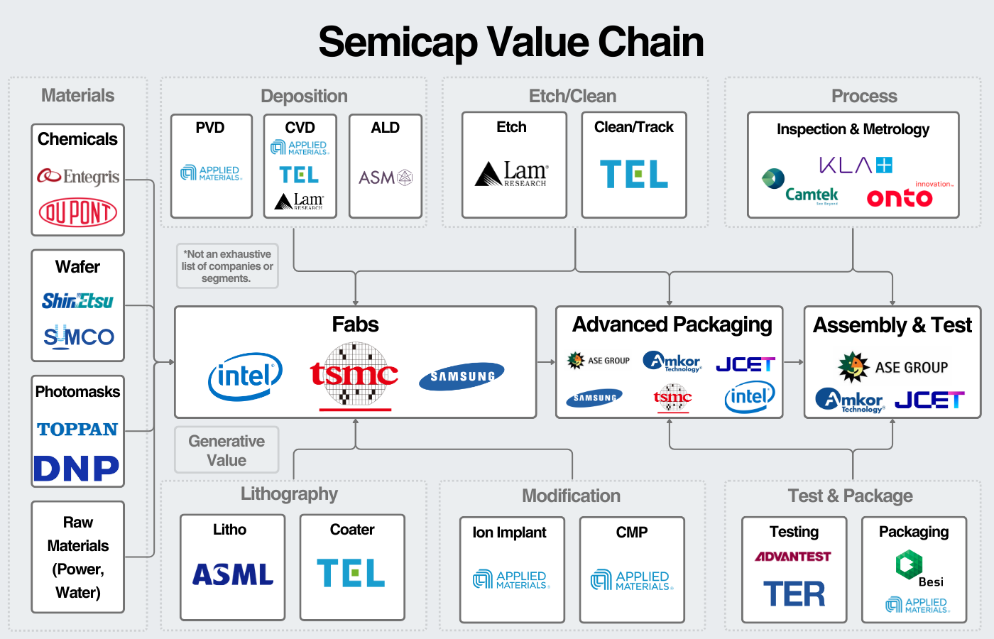
Other variables within that include demand for chips, the amount of chips being produced, and the complexity of those chips. We can see how value flows through the ecosystem here:
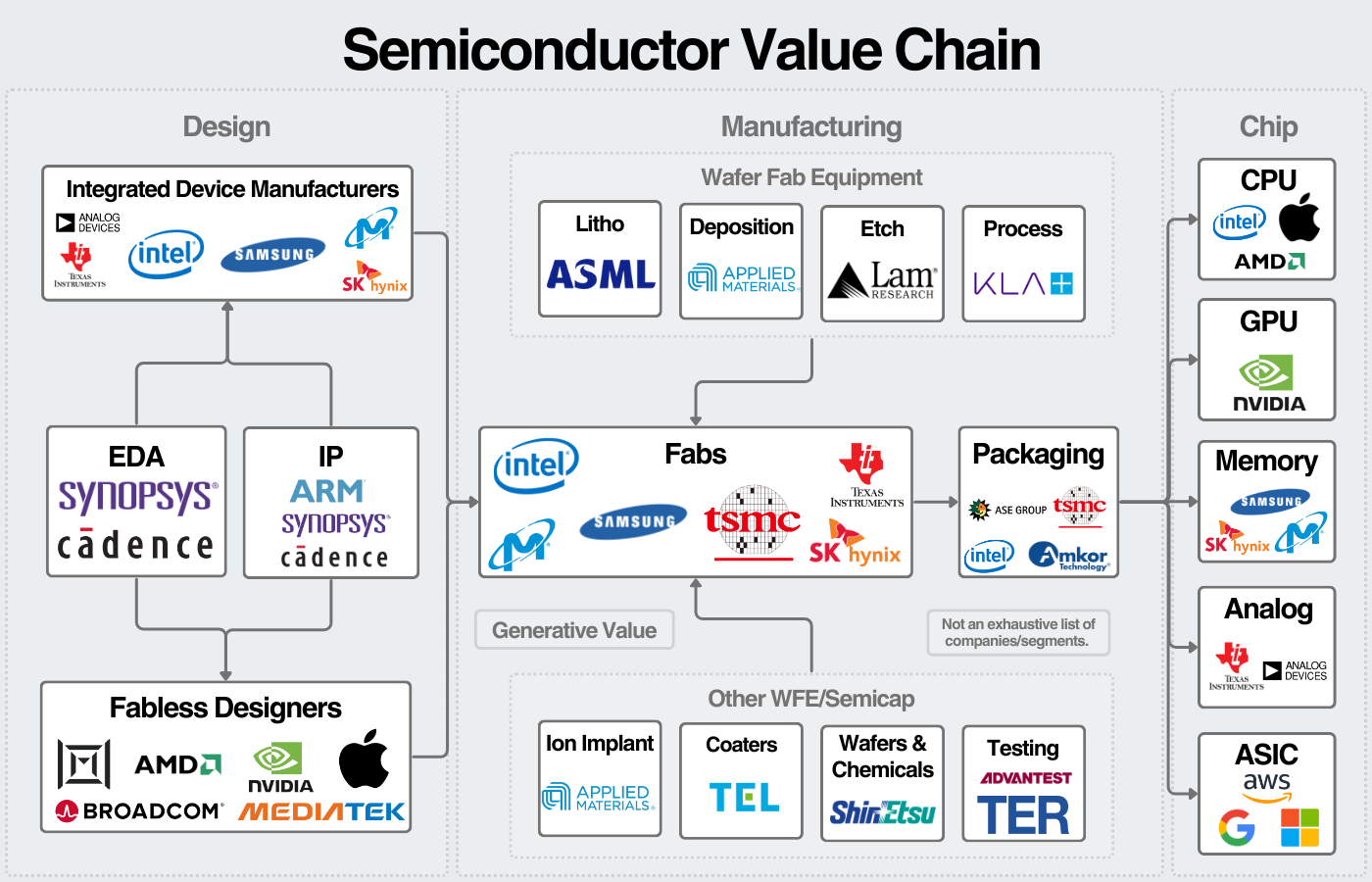
Fabless firms like Nvidia or AMD will design their chips and partner with foundries like TSMC/Samsung to manufacture them. Integrated Device Manufacturers (IDMs) will manufacture their own chips in their fabs.
Fabs need to buy hyper-specialized equipment for each stage of the manufacturing process and customize it for the specific semiconductor being manufactured.
This is a wonderful article on what that process looks like.
This leads to the manufacturing of five main types of chips: CPUs, GPUs, memory, analog, and ASICs. Here’s a semiconductor primer for more context.
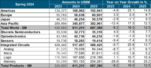
The relative market sizes can be found here (note that Memory was absolutely crushed last year but typically is the second largest market):
It’s also important to break down the industry by end market. The two largest markets for semiconductors are devices (smartphones/PCs) and data centers. Outside of that, industrial, automotive, and communications chips are large markets. For leading-edge nodes, TSMC gives us a good idea of where revenue comes from:
Tying these points together, the semicap industry is driven by end-user compute demand, which leads to chip demand, which leads to foundry demand, which ultimately leads to CapEx spent on semicap providers. The other note is that chip complexity and variation also help the semicap companies as the more complex a chip is, the more steps/equipment it requires for manufacturing.
2. Overview of Semicap and the Semiconductor Manufacturing Process
The semiconductor capital equipment companies provide the equipment necessary to manufacture, test, and package semiconductors.
Across this landscape, five major semicap companies generate a large percentage of the industry's revenue: ASML, Applied Materials, Lam Research, KLA, and Tokyo Electron.
Semiconductor Manufacturing
To understand the industry, we’ve got to break down the semiconductor manufacturing process.
I like the skyscraper analogy from Fabricated Knowledge. You build chips one floor at a time: design them, build them, tear away what you don’t need, finalize that floor, and build the next one.
At a high-level, this graphic from ASML is good to see the process:

The following steps are repeated until the base layer of the semiconductor is completed:
- Deposition: Materials are deposited onto the wafer, with specific characteristics based on the purpose of that step.
- Coating: The wafer is coated with a light-sensitive material called a photoresist.
- Lithography: The photoresist is exposed to light, projected through a reticle, which prints a specific pattern on the wafer.
- Etching: The wafer is baked and developed (like film). Etching then removes the necessary areas to provide the desired characteristics.
- Ion Implantation: Positive or negative ions may be “bombarded” onto the wafer to provide specific electric properties.
- Cleaning and polishing: Wafers will be frequently cleaned to remove any potential contaminants. A process called chemical mechanical polishing will then “polish” the wafer so it’s ready for another layer of materials
This will result in a wafer with transistors, capacitors, MOSFETs, wiring, and other electrical properties.
The early layers of this process are called “critical” where the transistors have the smallest features, the middle layers are called “semi-critical”, and the final layers are “non-critical.” This is important because the critical layers require the most complex machines, but the later layers might not.
Throughout this process, the machines and wafers will be tested frequently for defects. This is called metrology; if an error is found, it will be inspected to find a root cause. These tools are considered the “process control” piece of semicap.
The end result is a chip that looks like this:

The wafer looks like this:

After this wafer is completed, it needs to be packaged or cut into individual dies and attached to substrates. Another segment of packaging called advanced packaging includes techniques for packaging before cutting dies and packaging multiple chips onto one substrate. This (specifically a technique called CoWoS) has been a bottleneck for TSMC in leading-edge nodes. When TSMC’s CEO was asked about CoWoS in last quarter’s earnings call, here was his response:
“I also tried to reach the supply and demand balance, but I cannot today. The demand is so high. I have to work very hard to meet my customer's demands. We continue to increase. I hope sometime in 2025 or 2026, I can reach the balance.”
The overall goal of advanced packaging is to connect semiconductors in a way that improves performance without requiring smaller transistors. “Chiplets” are at the heart of this movement.
Finally, the chip will undergo testing and packaging. Historically, this was outsourced to outsourced assembly and testing (OSAT) companies; however, as packaging has gotten more complex, fabs have brought more and more of this functionality in-house.
Summarizing Chip Manufacturing
Semiconductors are made by depositing layers of materials onto wafers, projecting designs onto those wafers, etching away unnecessary components, and polishing the wafers. Each leading-edge semiconductor will require 1000+ steps before being ready for packaging.
Only a few firms in the world deliver the equipment necessary to complete the process, which we’ll discuss next.
3. Overview of Semicap Markets
For each of the techniques listed above, a number of more specialized tools complete those steps. For example, deposition includes physical vapor deposition, chemical vapor deposition, electrochemical deposition, and atomic layer deposition.
With that being said, ASML, Applied Materials, Lam Research, KLA, and Tokyo Electron are the market leaders in most of these categories (with a few exceptions like Atomic Layer Deposition). We can visualize their strengths here:

Top 5 Semicap Companies
Each of the major Wafer Fab Equipment (WFE) providers holds monopolies or oligopolies in specific verticals. See market share here (posted in 2023 but no major changes occurred):

1. ASML (Market Cap of ~$350B)
Market leader in lithography, a monopoly in cutting-edge machines. In large part, they’ve been responsible for pushing Moore’s law forward and transistor size down over the last decade.
2. Applied Materials (Market Cap of ~$174B)
“Do-it-all” equipment provider best known for deposition but also leads in CMP, Ion Implant, and advanced packaging equipment. Respectable positions in etch and metrology as well. AMAT offers the broadest portfolio in the industry and markets the “fab in a fab” strategy.
3. Lam Research (Market Cap of ~$120B)
Best known as the etch provider and a key enabler of the verticalization of memory chips. They’re seen as a beneficiary of the verticalization of logic chips as well:
Commentary from their CFO here: “When I look at the evolution of the architectures in most of the industry, things are going in the third dimension. That's largely what Lam Research does for the industry, right? When things go 3D, like NAND did a decade ago, our addressable market doubled for wafer.”
4. KLA Corp (Market Cap of ~$103B)
Process control giant with over 50% share in metrology and inspection. They analyze wafers for defects at each stage of the manufacturing process. They then aggregate that data to analyze where the defects are coming from, allowing the foundry to address those issues and increase utilization. Their business is driven by chip complexity, new fabs ramping up, more design starts (like custom chips), and end-market chip demand when companies need to maximize utilization.
5. Tokyo Electron (Market Cap of ~$90B)
Another “do-it-all” equipment provider. Their strongest position is in coaters where they have a near monopoly. We can see their market share across verticals here:
They further break down their positioning here:

To provide some more context, we can see revenue and market cap over time below.


The industry has delivered exceptional returns over the last decade, and this data doesn’t include dividends and stock buybacks which a company like AMAT has averaged ~5% a year. Several semicap companies have also committed to returning 80-100% of FCF to shareholders in the forms of dividends and buybacks.
This is mostly a positive thing, but it also shows there’s decreasing opportunities to reinvest capital at high rates of return. As Warren Buffett says,
"The best business to own is one that over an extended period can employ large amounts of incremental capital at very high rates of return.”
The industry has seen a level of consolidation and investment in the last decade that has led to unbelievable returns; it’s unclear to me how they could match those returns over the next decade. These businesses are more likely to be slower-growing, cyclical businesses that return a lot of cash to shareholders.
Industry Data
Two additional data points are important for individual semicap companies:
- Overall capital intensity of the industry
- Capital intensity of each semicap vertical
The capital intensity of the industry relative to overall semiconductor revenue has been one of the driving forces for growth over the last decade. Historically, the industry has made up 10-13% of semiconductor revenue; now, it’s at 15-16%. Lam’s CFO has the most candid commentary I’ve heard on the space:
”Okay, if semi revenue is $1 trillion, what is WFE? If I'm being honest with you, I don't know for sure. Capital intensity is going up, though. When I look at the cost of the most leading-edge wafers today in both NAND, in DRAM, in foundry and logic, it's going up per wafer. A planning metric or a thinking metric might not be unreasonable to think about 15% of revenue, might be higher, might be a little bit lower, largely doesn't matter.”
For leading-edge fabs, we can see WFE capital intensity here:

Within semicap, SemiAnalysis had a great graph highlighting the general size of each vertical here:

Of course, there are many companies I didn’t cover. ASM is the market leader in atomic layer deposition, BESI is an important player in advanced packaging, Entegris provides chemicals and filters to fabs. Each is an important player in the ecosystem. We can see all of those companies together here:

To summarize this section, the industry is dominated by 5 firms. Their success has mostly been driven by the overall growth of the semiconductor industry, the increasing capital intensity of semicap, and by individual company exposure to architecture inflections in semis.
4. Public Comps Data
We track the large semicap companies (in addition to large fabless firms, EDA software providers, and analog/memory providers).
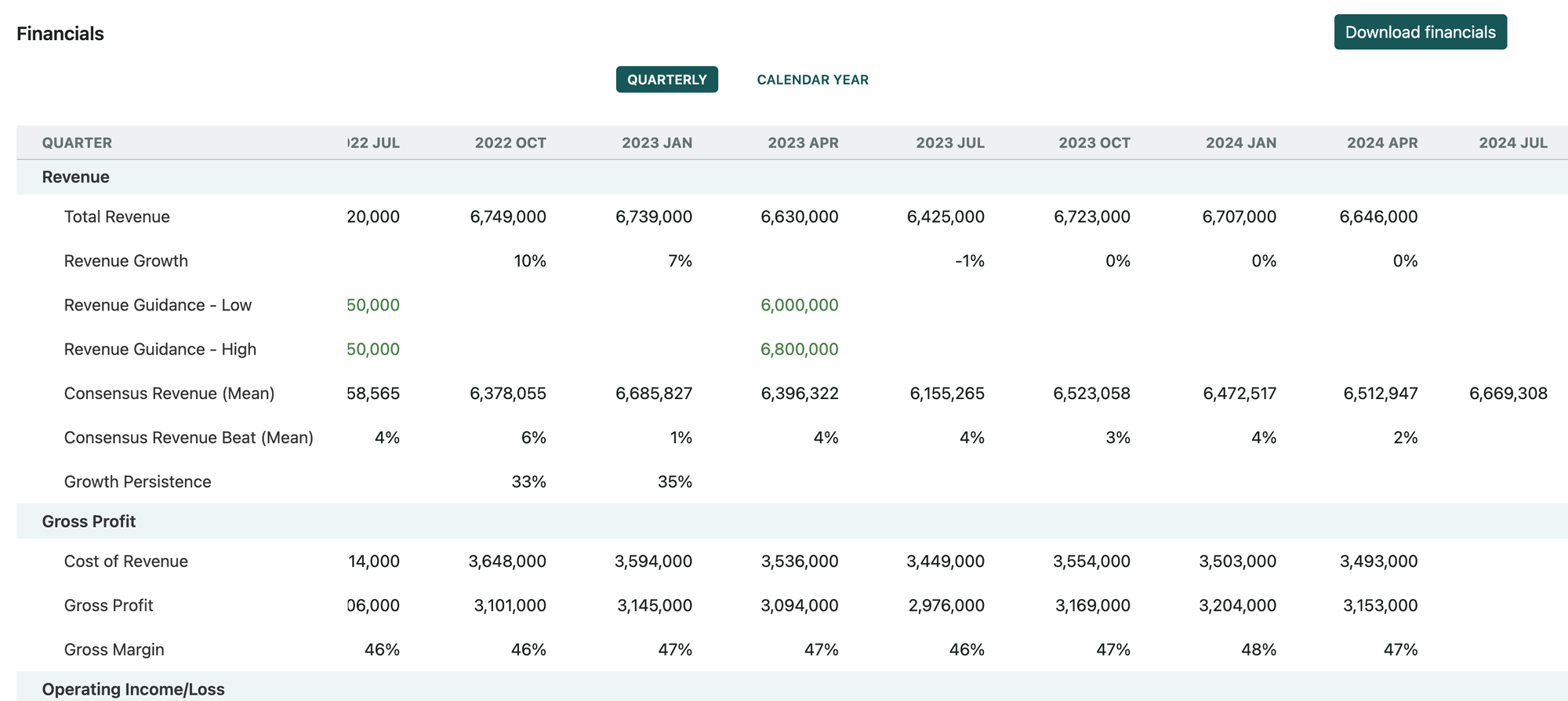
For example, Applied Materials financials:
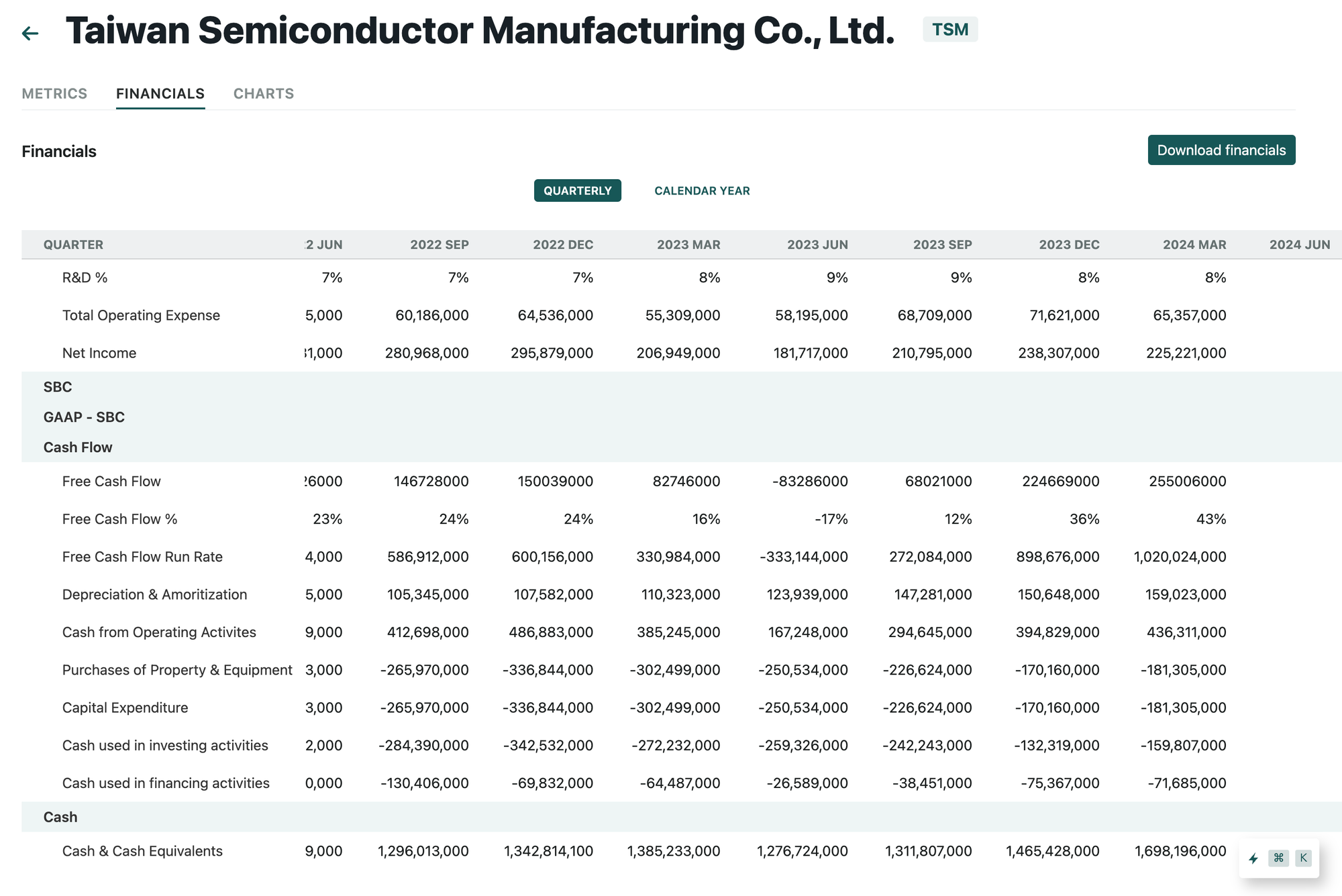
One of the most important metrics for the semicap space is TSMC's capex which can be seen here:
Feel free to reach out if there are specific companies you're interested in seeing data for.
5. Some Considerations for Investors
I typically end these articles with my thoughts on the industry (I can do that simply: I’m a believer in the space long-term, but a margin of safety is necessary due to its analytical difficulties).
Instead, I’ll discuss what I see are the key variables defining the industry over the next decade.
- Growing semiconductor end markets
First and foremost, the demand for computing must increase. New applications and demand for computing must arise. That, in turn, drives the amount and complexity of semiconductors manufactured. This then drives semiconductor capex, fab expenditures, and semi-cap purchases.
- Growing or flat semicap capital intensity
The core of this question comes down to the role semicap companies play in driving performance improvements. Lithography has been a defining variable pushing semiconductors forward over the last decade. The equipment driving these technology inflections will see the largest benefit.
- Semicap companies navigating the China threat
Revenue concentration, chinese competition, and government regulations all pose threats to the semicap companies. It will continue to be complex navigating this maze for the foreseeable future.
- Semicap companies navigating the current infrastructure buildout.
The industry has always been cyclical, and semiconductors are seeing a wave of demand right now. The industry must navigate the current infrastructure buildout so that it doesn’t pull forward the next 5-7 years of growth.
The final note is that this is a cyclical industry, which requires greater analytical rigor from investors and increases the importance of purchase price; patience is important.
My plan is to cover ASML, AMAT, KLA, and Lam Research in future articles.
As always, thanks for reading!
Disclaimer: The information contained in this article is not investment advice and should not be used as such. Investors should do their own due diligence before investing in any securities discussed in this article. While I strive for accuracy, I can’t guarantee the accuracy or reliability of this information. This article is based on my opinions and should be considered as such, not a point of fact. Views expressed are solely my own, not those of Public Comps or other employers.